Home > PCB Design > Xpedition Enterprise > Multi-Discipline Systems Engineering > Xpedition IC Packaging Solutions > Xpedition Substrate Integrator
Xpedition Substrate Integrator
Heterogeneous and homogeneous 2.5/3DIC Package Connectivity Planning, assembly prototyping, & system technology co-optimization
KEY FEATURES
2.5/3D IC Package Planning
Early prototyping and exploration allows engineers to evaluate different ASIC/chiplet, interposer, package, and PCB integration scenarios in order to meet overall PPA, device size, routability, and cost goals prior to detailed physical implementation.

Full or Partial Schematics Import
Package assembly logical connectivity can be constructed by using full or partial graphical schematics, useful for high device count designs such as SiP modules and/or the re-use/retargeting of previous designs.

System-level Package Connectivity Management
System connectivity management, visualization, and system-level logical verification of multi-die, multi-component, and multi-substrate IC package design.

Aggregation of Die, Chiplets & Substrates
Xpedition Substrate Integrator integrates die, chiplets, and interposers from different process nodes and suppliers. Multiple formats are supported including LEF/DEF, GDS, AIF, and CSV/TXT. Hierarchical virtual die models support bidirectional ECO changes of objects under design/optimization.

Silicon-package-PCB Cross Substrate Co-optimization
Cross-substrate planning and co-optimization greatly improve predictability during implementation by finding and fixing issues before they become late-stage surprises. A system perspective with cross-substrate visibility improves communication and coordination through immediate feedback to decisions typically made on an individual substrate basis.

Early Fast Signal Integrity Analysis
Provides an early exploration of SI performance during design planning and co-optimization allowing designers to explore multiple SI scenarios very early in the process while the cost of change is low. Prevents potential issues from reaching implementation causing delays and rework.

Comprehensive 3D Package Verification with Calibre
This verification solution provides extensive and comprehensive capabilities across every level of the package assembly through direct digital integration with Calibre 3DSTACK. By using the actual planned manufacturing data, as opposed to the design tools native database, you ensure that post-processing errors are not introduced.

System Connectivity Management
Construction and visualization of system-level logical connectivity of multi-die, multi-component, and multi-substrate IC package designs. Provides the ability to use System Verilog and graphical schematics to derive all or partial logical connectivity along with spreadsheet or interactive creation.
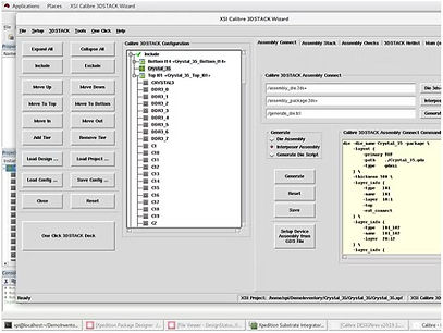
Calibre 3DSTACK
In conjunction with Calibre 3DSTACK, Xpedition Substrate Integrator uniquely identifies geometries per layer per die placement in the assembly, allowing accurate checking between dies. With the ability to differentiate the layers of interest per individual die placement, Calibre 3DSTACK enables designers to verify the physical attributes of each die.


Cross-Domain Interconnect Optimization
Visualization of the complete system in a single floorplan-in-floorplan view with flight lines or data-paths indicating connectivity between devices. Rules-based connectivity optimization can be run from any direction by signal, bus, or interface. Escape and breakout routing can be easily included to drive the System Technology Co-Optimization (STCO) process.
Tackling 2.5D Verification
These tools allowed us to detect out-of-sync connectivity between the design intent and the design implementation, preventing potential opens/shorts that could have occurred between the package and the PCB. If undetected, these errors could have created a costly time-consuming respin.
Company:eSilicon
Location:California, USA

HENISWARE
Henis Hardware Co., Ltd.
98/32 Moo 4, Bueng Yitho,
Thanyaburi, Pathumthani, Thailand
12130
+66 (0)2- 531-0997
+66 (0)87- 076 - 2484
